Wide-bandgap power at silicon cost – YESvGaN project develops competitive GaN process technologies
Can we contribute to the worldwide energy challenge by maximizing the efficiency in power conversion at a low cost? The answer is: YESvGaN! So, the goal of the YESvGaN consortium is to create a new class of vertical power transistors based on Gallium Nitride (GaN), so-called vertical GaN membrane transistors. These novel power devices combine the efficiency of wide-bandgap (WBG) semiconductors with the lower cost of the established silicon semiconductor technology. Within YESvGaN, the development of the required new technology all the way from wafer to application is covered.
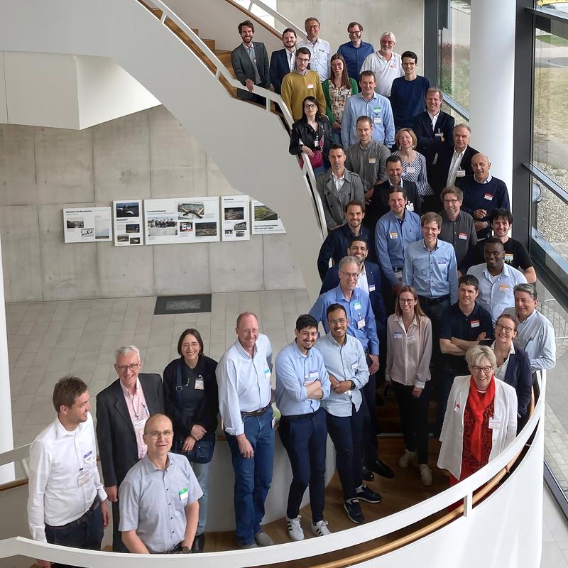
Since the project launched on May 1, 2021, impressive developments have been made by the project consortium, consisting of 23 European partners. Vertical device demonstrators with FinFET architectures and Schottky diodes – being important building blocks for a novel vertical membrane transistor technology – have been created successfully. Also, vertical layer stacks have been grown on silicon and sapphire with a diode breakdown voltage exceeding 500 V. This is a major step to reach the overall project goal of 1200 V blocking voltage on low-cost silicon or sapphire substrates. As a result, the market for future high-performance applications, e.g., in the automotive industry, could be accessible for the GaN semiconductor material.
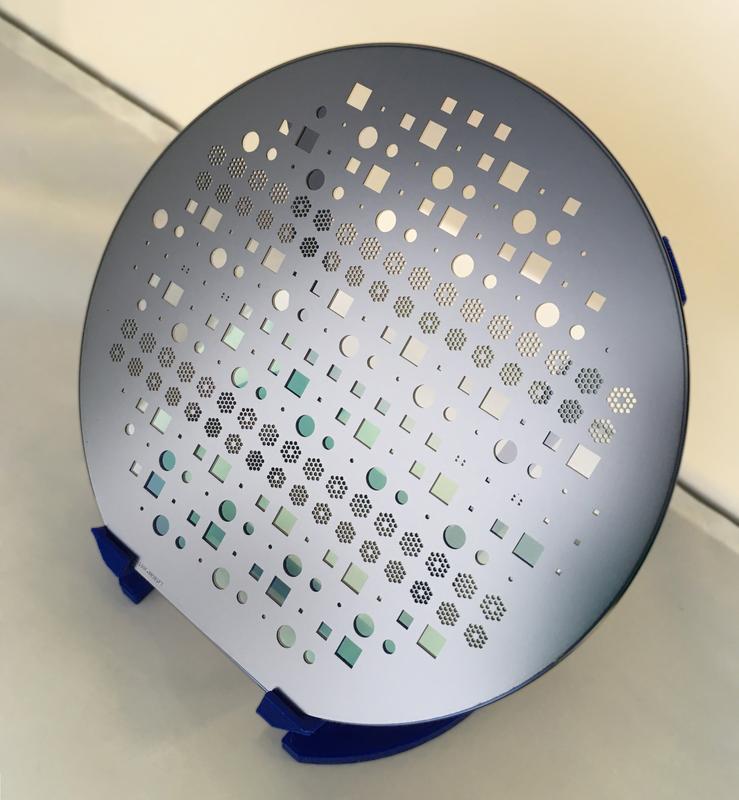
For vertical GaN power transistors with ultra-low resistance contribution from the backside contact, the development of a reliable membrane process technology is crucial. YESvGaN has succeeded in producing such fragile GaN membranes with a thickness of a few micrometers and a diameter of several millimeters without breaking. Novel assembly and interconnection technologies are being tested for the final application of membrane vertical GaN power transistors under extreme conditions. This includes operating temperatures of more than 250 ⁰C. In addition, virtual prototypes are being developed to evaluate the efficiency of GaN devices in the target applications using digital twins.
We are confident that YESvGaN will continue to achieve promising results in the next phases of the project and take a significant step towards fully vertical GaN membrane transistors.
So, can we contribute with energy-efficient low-cost vertical GaN technology to the worldwide energy challenge? Our answer remains: YESvGaN!
Wissenschaftlicher Ansprechpartner:
Dr. rer. nat. Elke Meißner
Group Manager GaN & AlN
Fraunhofer Institute for Integrated Systems and Device Technology IISB
Schottkystrasse 10
91058 Erlangen, Germany
Phone +49 9131 761 - 136
elke.meissner@iisb.fraunhofer.de
Weitere Informationen:
http://YESvGaN Project Homepage: https://www.yesvgan.eu/en
http://GaN & AlN activities and services at Fraunhofer IISB: https://www.iisb.fraunhofer.de/en/research_areas/materials/gan-aln.html
Ähnliche Pressemitteilungen im idw


