World record – OLED microdisplay with 10,000 dpi in 28 nm technology
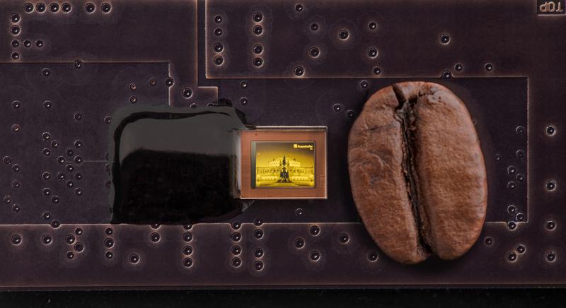
OLED microdisplays have been developed on 200mm wafers. These CMOS technologies and the design have limited the number and size of pixels. At the Fraunhofer Institute FEP, OLED microdisplays have been realized in a 28-nanometer backplane technology on 300mm wafers within the "Backplane" project funded by the Saxon State Ministry of Economics, Labor and Transport. Components with a display diagonal of 0.18 inches and pixel sizes of 2.5 micrometers have been manufactured. This corresponds to a pixel density of 10,000 dpi – an unattained level in the OLED microdisplay market. These OLED microdisplays will be presented at SID Display Week, May 23–25, 2023, in Los Angeles, USA.
In Silicon Saxony, the German location with world-leading microelectronics and semiconductor manufacturers as well as research institutions, work on forward-looking innovations is carried out daily. Fraunhofer FEP, as part of this closely interlinked network, is the leading institute for the development of customer- and application-specific microdisplays and sensors based on OLED-on-silicon technology.
The institute's continuous microdisplay developments in recent years have been driven by various requirements such as pixel density, energy efficiency, color, brightness, or frame rate. Fraunhofer FEP has developed a wide range of microdisplays in full-color or monochrome, from ultra-low power versions to high-resolution variants for the use in augmented- (AR) and virtual-reality (VR) applications and other wearables.
The majority of microdisplays on the market are currently developed and manufactured on 200 mm wafers in 250 nm to 90 nm CMOS process nodes. At Fraunhofer FEP, too, these are established design technologies in cooperation with various semiconductor manufacturers, depending on the requirements and customers' wishes. The manufacturing of microdisplays on 300 mm wafers has been rare so far. On the one hand, this is due to technical reasons, such as the availability of suitable transistors for the corresponding control of the OLED, and on the other hand to economic reasons.
However, market requirements for image quality, pixel density and integrated functionality are continuously increasing. Therefore, Fraunhofer researchers have been examining the scaling effects in smaller CMOS technologies and investigating the use of 300 mm backplane processes as part of the "Backplane" project funded by the SMWA. In this context, the researchers have now succeeded in making the next major leap forward in development: For the first time, they realized an OLED microdisplay with tiny 2.5 µm pixels (corresponding to 10,000 dpi) at a display diagonal of 0.18 inch. This demonstrated the feasibility of developing displays based on 28 nm small-node technology on 300 mm wafers and realized the world's smallest pixels of an OLED microdisplay.
Philipp Wartenberg, head of the department for IC and system design, explains the new technology: "In so-called "small node" technologies, there is always the challenge of realizing the voltages required for driving in complex photonic systems. Thanks to an interdisciplinary research team and a completely new type of display architecture, we have succeeded in doing this for the first time in this project, while at the same time realizing extremely small pixels with a size of just 2.5 µm. Thanks to this very important development step, we will be able to offer an even greater development scope to our customers and partners in the future, with an even higher resolution on a smaller area. In addition, the small node technology enables novel control concepts that further reduce power consumption, which is important for mobile applications. We were able to demonstrate this, for example, through a demand-oriented, flexible control method as well as a scalable architecture."
The newly developed OLED microdisplays have a resolution of 1440 × 1080 pixels in monochrome or 720 × 540 pixels in full color. On the one hand, the flexible display architecture allows the refresh rate to be reduced to 0 Hz in extreme cases when the display content remains unchanged, thus avoiding all unnecessary data transfer - an enormous advantage for power consumption. Conventional displays require a minimum refresh rate here, regardless of content. On the other hand, the new microdisplay also allows frame rates of up to 480 Hz in extreme cases - internally even up to several kHz. This has been made possible by a programmable sequence control in combination with a display-integrated frame buffer.
Depending on the design, the new displays can be used in lifestyle products such as sports glasses or as head-mounted displays in motorcycle helmets, in industrial scenarios for wearables in logistics or for remote maintenance solutions. The now even smaller dimensions pave the way for even more ergonomic systems.
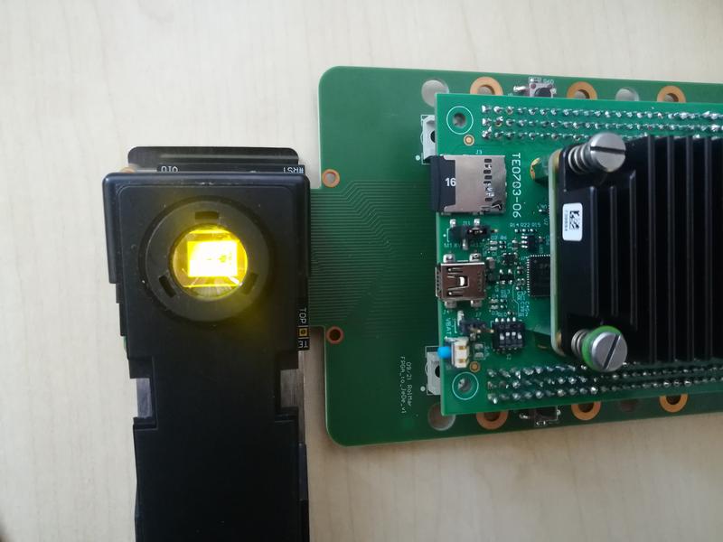
The new OLED microdisplays will be offered by Fraunhofer FEP as evaluation kits to provide interested customers with access and testing opportunities for their own system integration and to enable joint customer-specific microdisplay developments with industry. They will also be presented live for the first time at the SID Display Week 2023, May 23 – 25, 2023, in Los Angeles, USA, at the German joint booth at Fraunhofer FEP, booth #1110, and in corresponding presentations.
About the project „Backplane“
Backplane – Deep-submicron CMOS process technology for driving integrated
microdisplays and evaluation circuits of optical sensors
Funded by: Saxony State Ministry for Economic Affairs, Labor and Transport
Funding reference: 100392259
Duration: 31.12.2019 – 31.10.2022
Fraunhofer FEP at SID Display Week 2023
May 23 – 25, 2023
Los Angeles, USA
German Pavilion, booth no. 1110
www.displayweek.org
Talks and Presentations
Tuesday, May 23, 2023:
Session 3: Emerging Technologies and Techniques I (Emerging Technologies and Applications)
11:10 - 12:30 am / room 304ABC
3.4: Invited Paper: A 2.5μm Dot Pitch 0.18” OLED Microdisplay on 28nm CMOS Backplane
Philipp Wartenberg, Fraunhofer FEP
Session 19: Holographic and 3D Optics (Emerging Technologies and Applications)
3:40 pm - 5:00 pm, room 402AB
19.3: Slim Backlights for Holographic 3D Displays by Advanced Coatings Capabilities
Ullrich Hartung, Fraunhofer FEP
Exhibitor Forum
Wednesday, May 24, 2023
Session: AR/VR, Presentation Number: F6.3
09:45 am
A 2.5μm Dot-Pitch 0.18-in. OLED Microdisplay on 28nm CMOS Backplane
Andreas Fritscher, Fraunhofer FEP
Press contact:
Ms. Annett Arnold
Fraunhofer Institute for Organic Electronics, Electron Beam and Plasma Technology FEP
Phone +49 351 2586 333 | presse@fep.fraunhofer.de
Winterbergstraße 28 | 01277 Dresden | Germany | www.fep.fraunhofer.de
Weitere Informationen:
https://s.fhg.de/7h3
Ähnliche Pressemitteilungen im idw


