
Gallium nitride plays a key role in greener electronics
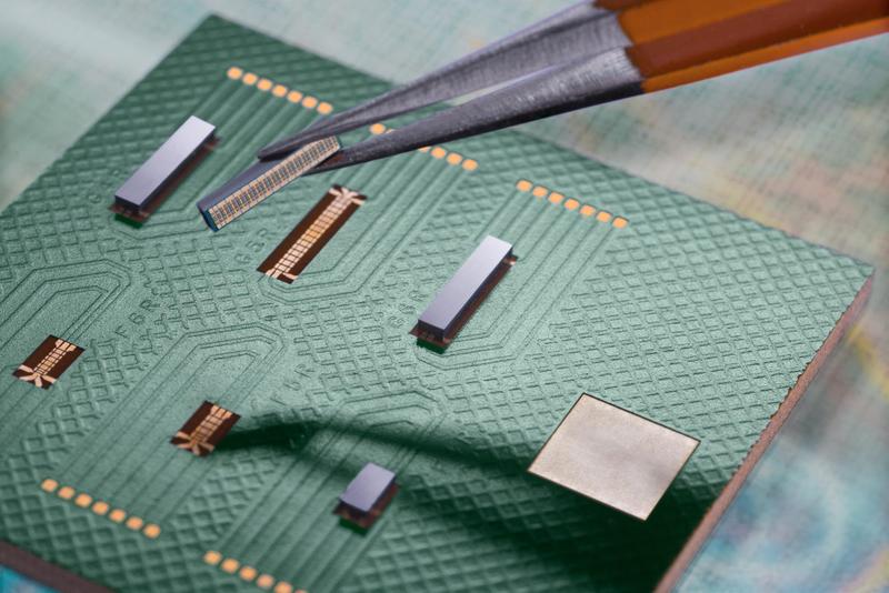
A significant reduction in energy consumption and CO₂ emissions through modular and easy-to-integrate GaN power semiconductors – this is the objective of the EU-funded All2GaN project. Forty-five partners from twelve countries are collaborating to unlock the energy-saving potential of gallium nitride (GaN) semiconductors for a broad range of industrial applications. Fraunhofer IZM plays a key role across the value chain: leveraging its internationally recognized expertise in packaging technologies, the institute is developing innovative assembly solutions that are essential for the performance, miniaturization, and sustainability of next-generation GaN electronics.
Gallium nitride is regarded as one of the most promising semiconductor materials for future electronic systems. Compared to silicon, GaN enables higher power densities, lower switching losses, and higher operating frequencies – providing decisive advantages for applications in telecommunications, data centers, e-mobility, renewable energy, and smart grid technologies.
The components developed within the All2GaN project (“Affordable smart GaN IC solutions for greener applications”) are being evaluated in eleven industrial use-case demonstrators to systematically assess their efficiency potential. Across all use cases, the researchers expect to achieve an average reduction in power losses of around 30 percent. In addition, the project aims to establish an integration toolbox that will pave the way for a new generation of modular, easy-to-integrate GaN power semiconductors.
The development of suitable interconnection technologies for printed circuit boards is essential to fully exploit the advantages of gallium nitride in real-world applications. While other project partners are investigating conventional soldering approaches and sintering technologies, the scientists at Fraunhofer IZM are focusing on thermocompression – a process particularly well suited for fine-pitch applications with dimensions below 10 µm.
𝐍𝐚𝐧𝐨𝐩𝐨𝐫𝐨𝐮𝐬 𝐠𝐨𝐥𝐝 𝐚𝐬 𝐚 𝐠𝐚𝐦𝐞-𝐜𝐡𝐚𝐧𝐠𝐞𝐫 𝐟𝐨𝐫 𝐟𝐢𝐧𝐞 𝐬𝐭𝐫𝐮𝐜𝐭𝐮𝐫𝐞𝐬 𝐚𝐧𝐝 𝐫𝐞𝐥𝐢𝐚𝐛𝐥𝐞 𝐢𝐧𝐭𝐞𝐫𝐜𝐨𝐧𝐧𝐞𝐜𝐭𝐢𝐨𝐧𝐬
A central role is played by the nanoporous gold (NPG) developed at Fraunhofer IZM. It consists of a three-dimensional network of nanoscale gold ligaments created through the selective dissolution of silver from a gold-silver alloy. As the miniaturization of microelectronic systems continues to advance, NPG is increasingly attracting attention as a promising material for next-generation assembly technologies.
NPG is considered a highly promising alternative to conventional joining methods, opening up new possibilities for reliable assembly technologies. It enables solder-free interconnection for direct chip attachment on organic printed circuit boards and, thanks to its sponge-like structure, provides a significantly broader process window than traditional soldering approaches. Its unique deformation behavior allows for highly precise and dependable connections even within extremely confined spaces. At the same time, the porous structure efficiently compensates for relatively large topographical variations between the joining partners. Another major advantage lies in the material’s exceptionally large specific surface area, which enables material-bonded interconnections at comparatively low temperatures. This considerably reduces thermal stress on sensitive components.
As a result, nanoporous gold is emerging as a forward-looking material for high-precision applications, particularly in areas where conventional soldering technologies are approaching their physical and technological limitations.
𝐆𝐫𝐞𝐚𝐭𝐞𝐫 𝐞𝐟𝐟𝐢𝐜𝐢𝐞𝐧𝐜𝐲 𝐚𝐧𝐝 𝐬𝐮𝐬𝐭𝐚𝐢𝐧𝐚𝐛𝐢𝐥𝐢𝐭𝐲 𝐭𝐡𝐫𝐨𝐮𝐠𝐡 𝐢𝐧𝐧𝐨𝐯𝐚𝐭𝐢𝐯𝐞 𝐦𝐚𝐭𝐞𝐫𝐢𝐚𝐥 𝐚𝐧𝐝 𝐬𝐲𝐬𝐭𝐞𝐦 𝐚𝐩𝐩𝐫𝐨𝐚𝐜𝐡𝐞𝐬
In addition to technological innovation, sustainability is a central focus of the project. All2GaN forms part of the European strategy to support the objectives of the Green Deal by developing energy-efficient and resource-saving technologies.
GaN-based circuits can make a direct contribution to reducing energy consumption by minimizing power losses. At the same time, advanced packaging approaches – such as the use of nanoporous gold – enable more material-efficient integration while also extending component lifetime.
The projected energy-saving potential is substantial: with the widespread adoption of GaN-based circuits, around 86 TWh of energy could be saved annually within the EU alone over the long term. This corresponds to approximately 43 megatons of CO₂ emissions per year. On a global scale, the savings potential could reach 218 megatons of CO₂ annually – roughly equivalent to the yearly emissions of a medium-sized industrialized nation such as Spain.
The All2GaN project runs from May 1, 2023, to October 30, 2026, and is funded with a total budget of €60 million under the Chips Joint Undertaking (Grant Agreement No. 101111890). This includes €4.81 million provided by the German Federal Ministry of Research, Technology and Space (BMFTR) and €40,000 from the Free State of Thuringia.
(Text: Lotta Jahnke)
Wissenschaftlicher Ansprechpartner:
Juliane Fröhlich
Fraunhofer Institute for Reliability and Microintegration IZM
Research Assistant
Phone. +49 30 46403-676
juliane.froehlich@izm.fraunhofer.de
Originalpublikation:
https://www.izm.fraunhofer.de/en/news_events/tech_news/all2gan.html
Weitere Informationen:
https://www.all2gan.eu/home
Ähnliche Pressemitteilungen im idw